We study the electronic properties of 2D materials using twistronics, straintronics and slidetronics principles. Adjusting the twist angle, applying mechanical stress and manipulating the stacking order of crystalline materials can greatly influence their electronic properties. Through these correlation-engineering techniques, we aim to manipulate the properties of stacked 2D materials and explore their various quantum ground states such as superconductivity, magnetism and topology. To this end, we will develop custom, state-of-the-art setups that can manipulate crystalline matter at will (such as the QTM below) and to characterize them (magneto transport).
Quantum Twisting Microscope
Quantum Twisting Microscope (QTM) is a revolutionary invention that allows continuous in-situ twisting for the purpose of 1. tuning the twist angle between two neighboring layers and 2. probing the band structure of the underlying sample through the momentum-energy resolved tunnelling spectroscopy. We aim to build a cryogenic version of the QTM. Read more about it from the original inventors, and my former group in Munich.

Magneto Transport
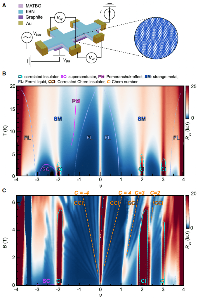
Twisting two sheets of 2D materials is an entirely new tuning knob that brings new emergent states that are not seen in the native state of the material. On the right is an example of a magic angle twisted bilayer graphene (MATBG) sample which is two layers of graphene with ~1.1 deg of twist angle between them. This causes 1. Moire periodic potential pattern and 2. flat band near the Fermi level to emerge which hosts various correlated phenomena such as superconductivity, correlated insulator and magnetism. We are able to fabricate high quality twistronics devices using advanced van der Waals assembly techniques such as cut-and-stack and edge-clamping techniques. Read more about it here.
Methods, Techniques, Tools we use
These are the procedures, techniques and methods we use on a day to day basis:
- Nanofabrication
- Exfoliation of 2D materials
- Van der Waals assembly into clean heterostructures
- Optical/e-beam lithography to structure the device into optimal shape
- Physical vapour deposition
- Dry/Wet Etching
- Focused ion beam induced deposition
- Wirebonding
- Characterization
- Raman/Photoluminescence spectroscopy
- Atomic Force Microscopy
- Optical microscopy
- Scanning electron microscopy
- MagnetoTransport
- Cryogenics
- Active/passive signal processing
- Low noise measurements
- Quantum Transport
- Quantum Twisting Microscope
- Room temperature
- Low temperature
- Scanning probe microscopy
- In-situ twisting
- Strain engineering
- In plane tension
- Out-of-plane pressure
- Designing and building custom lab equipment
- Low noise circuit
- Signal processing
- PCBs and optimal sample geometry
